6.5 kV SiC Full-Bridge Power Module: Technical Study
An in-depth analysis of a medium-voltage SiC MOSFET module for megawatt EV charging: packaging, parasitic inductance, switching tests and the limits the paper leaves open.
THE STORY
For a Master 1 SAIETI oral at Université Paris-Saclay, I studied Boutry et al., "A 6.5 kV Full-Bridge SiC MOSFET Module Design" (IWIPP 2025, University of Alabama) in depth and rebuilt its key ideas as my own diagrams: why medium-voltage applications need SiC, how a full bridge fits in an XHP3 footprint, how the module is built, and how it was tested. I then added my own critical analysis of what the results do not yet show, with first-order calculations and a simulation plan I intend to carry out. This is a study of published work, not hardware I built.
MY CONTRIBUTIONS
- Redrew the topology, fabrication sequence, die-attach metallurgy, wire bonding and double-pulse test as original diagrams.
- Explained why the commutation inductance curves fall with frequency (flux cancellation, skin and proximity effects).
- Compared the sub-scale prototype (2.5 kV, 11 A, FR4/ABS/Al) with the full-scale target (4 kV, 40 A, AlN/PEEK/AlSiC).
- Raised issues not discussed in the paper: Sn63Pb37 solder melts at 183 °C against a 175 °C die rating, and the turn-on ringing has EMI consequences.
- Added an ethical, social and environmental assessment (lead in solder, energy-intensive SiC wafers, high-voltage safety).
- Bounded the turn-off di/dt from the reported overshoot (ΔV ≈ L·di/dt gives under ~5.8 A/ns) and planned an LTspice double-pulse study of loop inductance and gate resistance.
What the paper proposes
Two identical half-bridge substrates in one XHP3 housing give a 6.5 kV SiC full bridge. Joining the two midpoints turns it into a half bridge with twice the current, so one module serves both topologies.
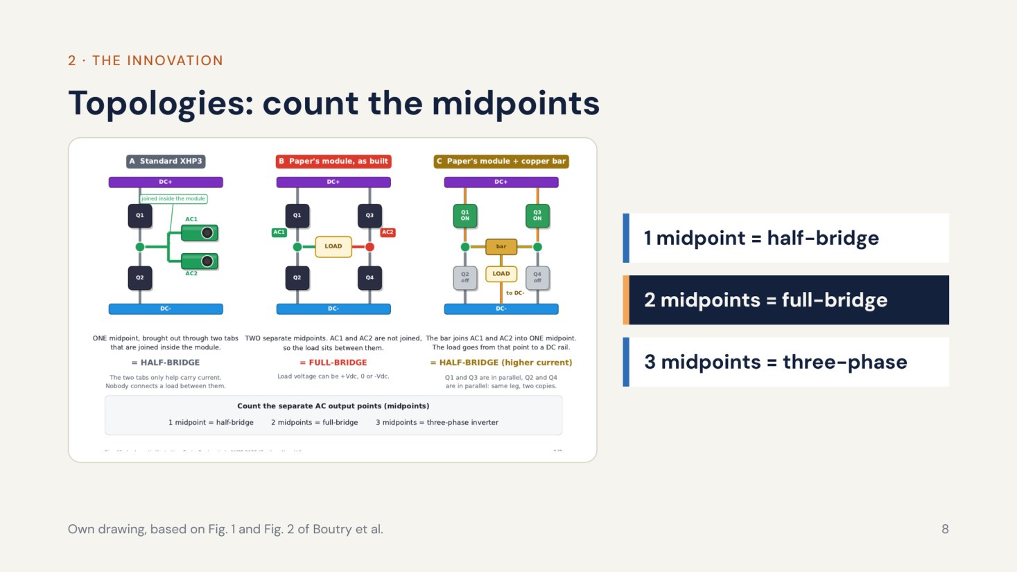
Topologies: count the midpoints (own drawing)
The problem
Megawatt EV charging, 3.3 kV+ rail traction and solid-state transformers need higher voltage, smaller size and higher power density. SiC (3.3 eV bandgap against 1.1 eV for silicon) blocks more voltage with lower losses, but very few packaged SiC modules exist above 3.3 kV: a bare die is not a product.
How it is built
The steps are: Sn63Pb37 reflow die attach, 20-mil aluminium wire bonds, MCX gate connectors with a 5 Ω gate resistor, substrates mounted on an aluminium baseplate, copper terminals soldered in a jig, then a 3D-printed ABS housing.
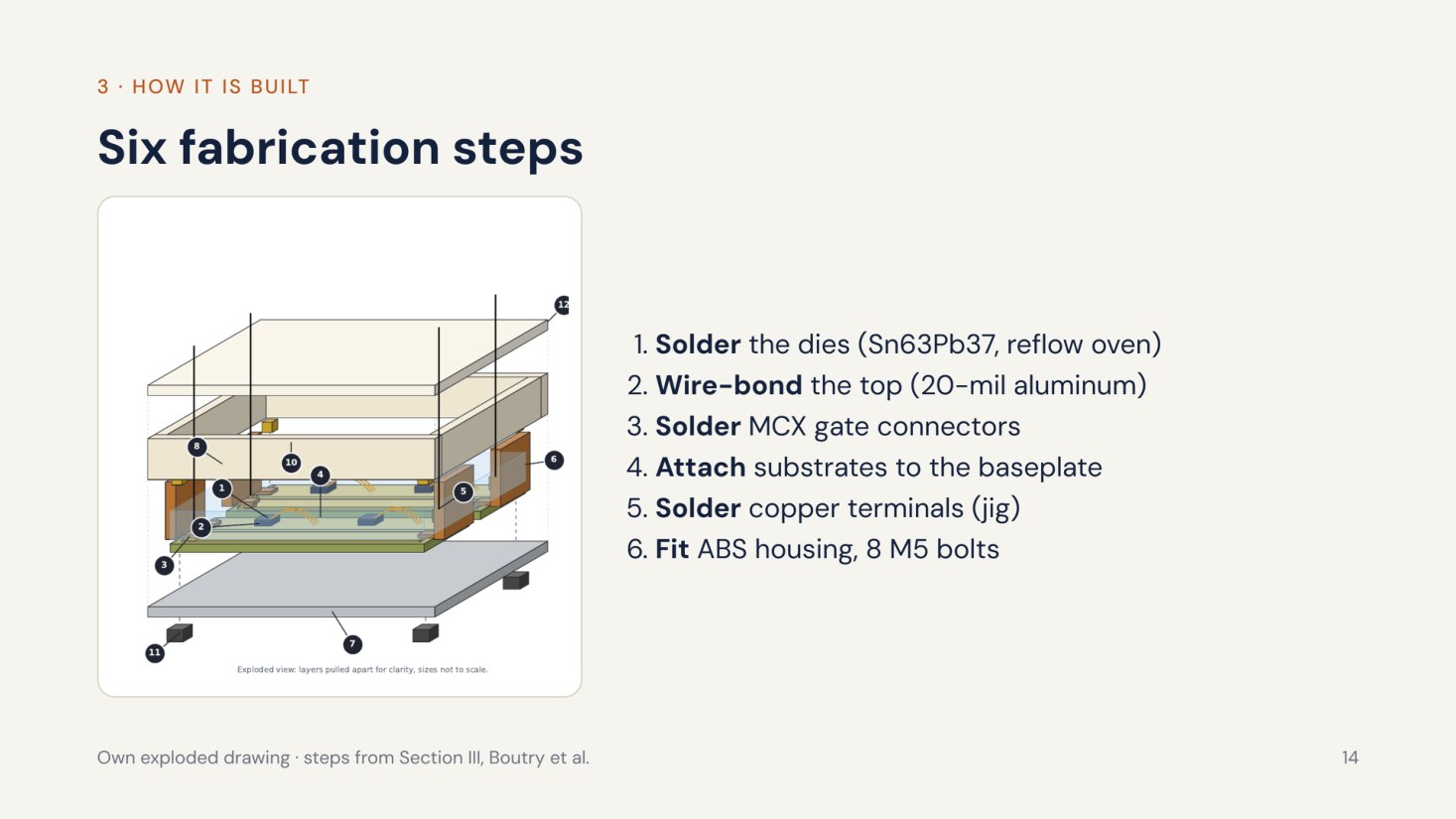
Six fabrication steps (own exploded drawing)
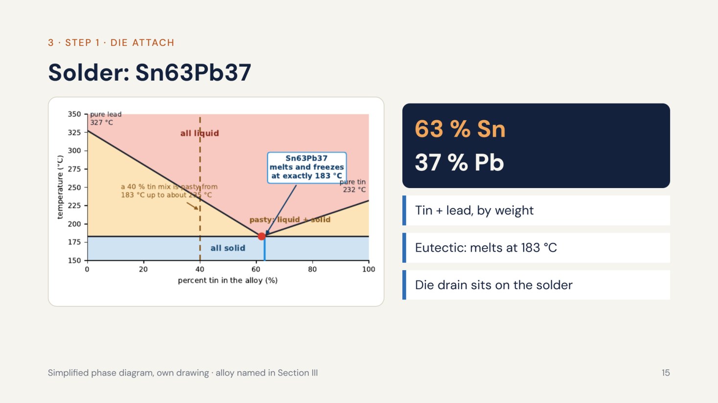
Sn-Pb phase diagram: eutectic at 183 °C (own drawing)
Up close: parasitic inductance
The paper reports a Q3D-extracted commutation inductance of 34.5 nH (target 20 nH) with balanced legs (45/46 nH). I explained why the curves fall with frequency: opposite currents in close plates cancel flux, and skin and proximity effects push current to the facing surfaces. Larger DC-plate overlap is the fix the authors propose.
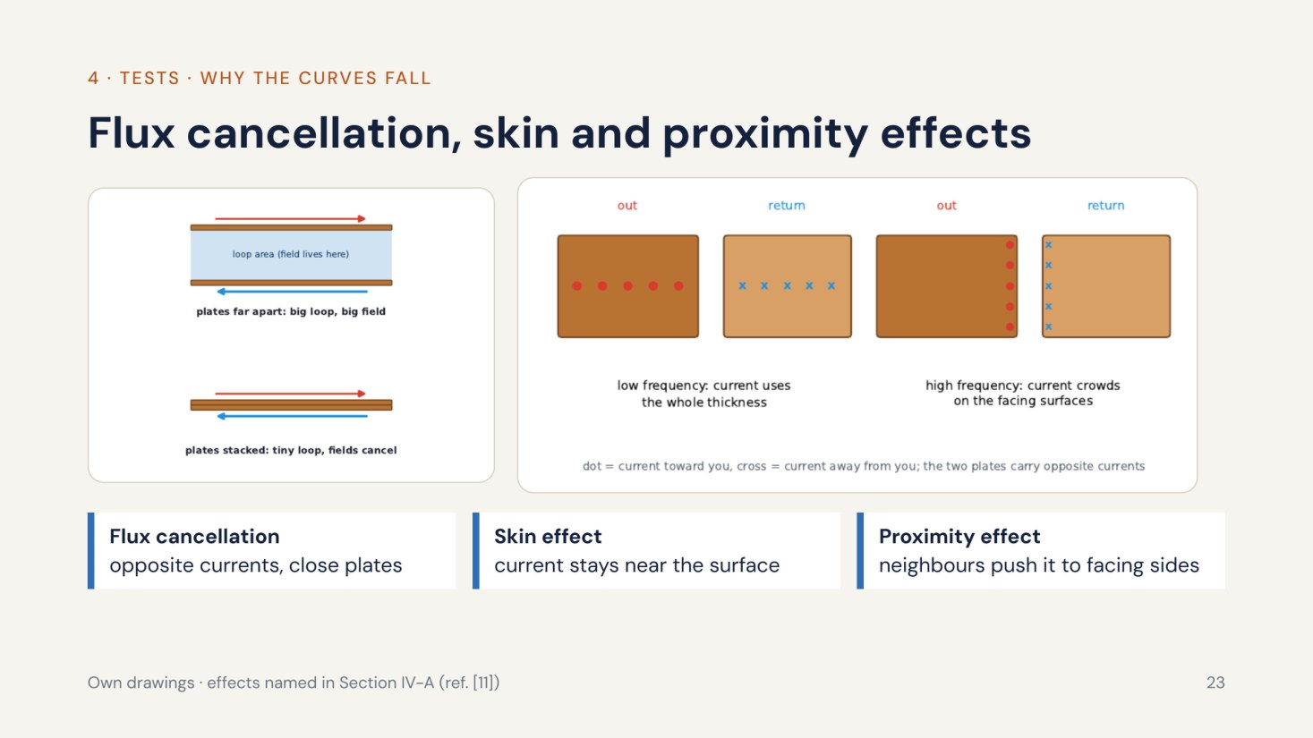
Flux cancellation, skin and proximity effects (own drawings)
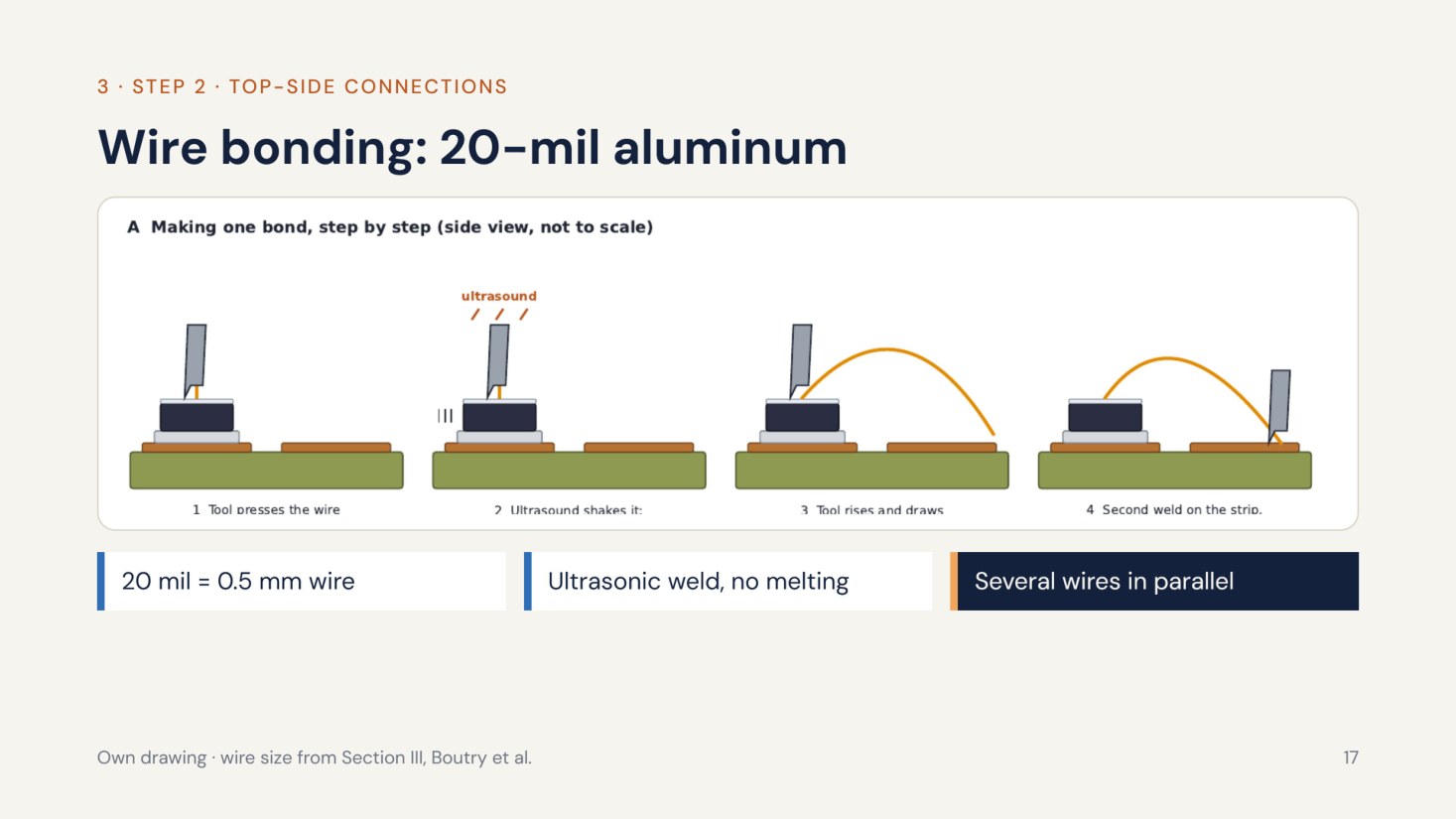
Wire bonding: 20-mil aluminium (own drawing)
Under the hood: the tests
Static: a Keysight B1505A curve tracer measured about 300 mΩ on-resistance and leakage up to 3.0 kV. Dynamic: a double-pulse test at 2.5 kV, 10 A, 5 Ω and 25 °C showed turn-off overshoot under 200 V and turn-on current ringing peaking near 44 A.
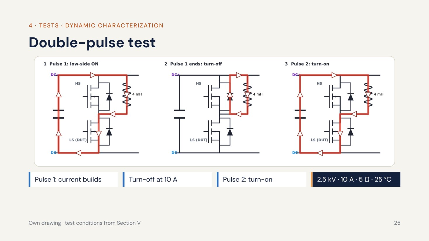
Double-pulse test sequence (own drawing)
Limits and open issues (my analysis)
Several limits remain. The inductance is 34.5 nH against a 20 nH target. Strong turn-on ringing is an EMI source. The tests stop at 2.5 kV, 10 A and 25 °C, and leakage was measured only to 3.0 kV of 6.5 kV. Partial discharge is untested, the prototype uses FR4 and ABS, and the eutectic solder melts at 183 °C while the die is rated to 175 °C, which leaves little thermal margin for the full-scale module.
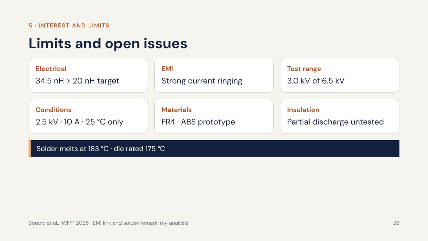
Limits and open issues
Beyond the lab
On the environmental side, higher efficiency and faster EV charging are gains, while lead in the solder and energy-intensive SiC wafers are costs. On the social side, faster EV adoption comes with high-voltage safety and training needs. On the ethical side, reliability, honest reporting of limits and a responsible supply chain all matter.
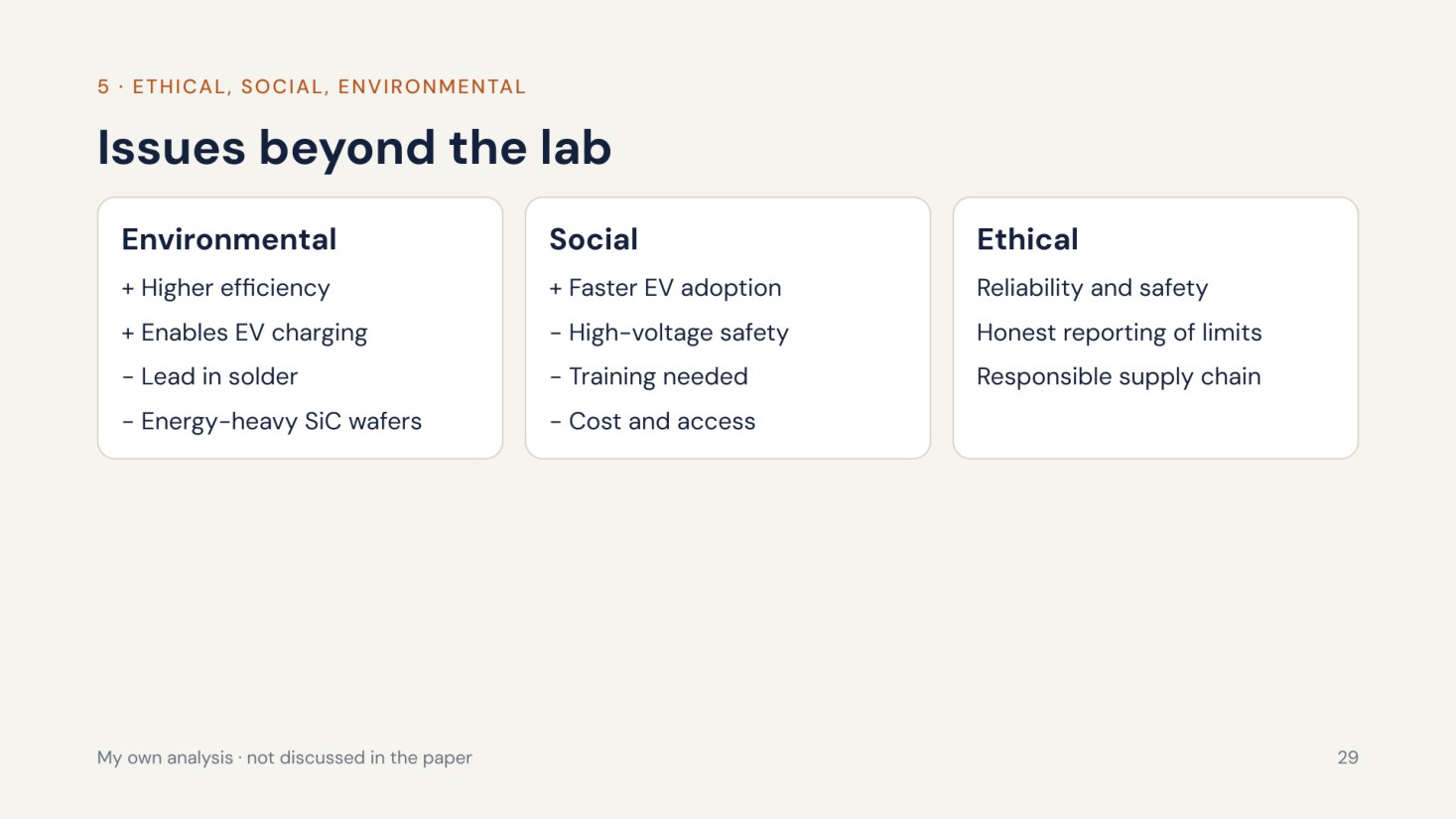
Ethical, social and environmental assessment (own analysis)
Reflection / what I learned
Packaging, not the die, sets the limits at medium voltage: loop inductance, insulation and thermal margins decide whether a 6.5 kV chip becomes a usable module. This is the research area I want to work in: reliable, low-parasitic medium-voltage SiC power conversion.